Yale Institute for Nanoscience and Quantum Engineering (YINQE)
Building: Malone Engineering Center, 55 Prospect St, rm 003
About the core
The Yale Institute for Nanoscience and Quantum Engineering (YINQE) is a shared core facility for electron microscopy, atomic force microscopy, and electron-beam lithography. Graduate students, undergraduates, postdocs, and faculty have hands-on access to all instruments.
- Scanning electron microscopy: Hitachi SU-70 SEM w/ Oxford EDS Ultim Max Infinity 170
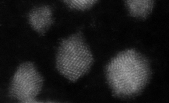
- Transmission electron microscopy: FEI Tecnai Osiris 200kV TEM
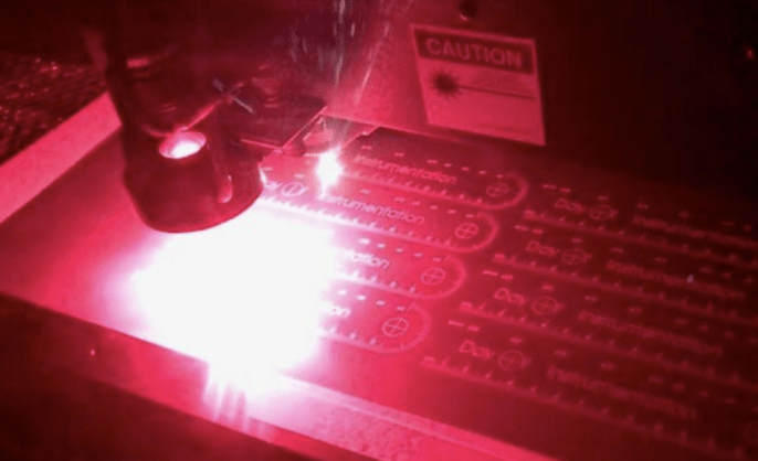
- Electron-beam lithography: Raith EBPG 5000+ and EBPG 5200+
- Atomic force microscopy: Bruker Dimension Fastscan AFM
- X-ray diffractometry: Rigaku Smartlab XRD
Available to Yale researchers & external researchers
Core websiteApply for an account
YINQE has transitioned to a new Core Facility Management System, PPMS.
Yale people
Create your PPMS account by visiting YINQE@PPMS.
Request authorization to financial accounts (COAs); details in the Quick Start Guide.
Outside users
Fill out form in the External Customer System.
Email YINQE so that we can set up your account. You are required to submit an additional form, called the Memo Of Understanding, and to provide an insurance rider described in that form.
Everyone
Please use YINQE@PPMS to request training. Once your PPMS account is set up, please go to the Request tab and fill out the “New to YINQE?” form.
How to enable instruments: details on the User Setup Guide-Enabled Instruments.
Schedule training
We have developed video-based training courses for all instruments in the YINQE lab. (YINQE@YouTube)
Lab access
If you are not already a registered YINQE lab user or need lab access, please complete the form using New to YINQE@YINQE PPMS.
SEM training
We have recorded a set of video clips for SEM training. You will be at the SEM, watching and copying the videos, while the instuctor is nearby and available for questions. You will stop the videos at various times so that the instructor can check your progress. This seems to work pretty well, and people like going through the course at their own pace. You might take one hour, or you might take four hours. It’s up to you.
Sign up for SEM training by using SEM training@YINQE PPMS.
TEM training
We have recorded a set of video clips for TEM training. It’s the same idea as our SEM training (see above.) Sign up for TEM training by using TEM training@YINQE PPMS. The hard part of TEM training is showing you how to use the load lock. But we found a way! The Gibbs shop made us a “load lock simulator” that lets you practice without abusing the vacuum pumps. Neat!
AFM training
We have recorded a set of video clips for AFM training. It’s the same idea as our SEM training (see above.) Sign up for AFM training by using AFM training@YINQE PPMS.
e-beam lithography training
e-beam training starts with an online course, which covers machine hardware, CAD, data preparation, and job setup. Send a request to e-beam lithography training@YINQE PPMS to get started with the online course. After you complete the course, you will do hands-on training with the EBPG e-beam system, using a video-based course similar to the ones used for SEM and TEM.
Microtome training
We have recorded a set of video clips for microtome (diamond knife) training. It’s the same idea as our SEM training (see above.) Sign up for microtome training by using Microtome training@YINQE PPMS. Your group will have to purchase a diamond knife. Glass knives will not cut the mustard, so don’t even think about it. If you need just one sample, then you should go to the Medical School or to an outside service. This course covers the simplest procedure, using epoxy embedding and room-temperature slicing. For instruction on staining and low-temperature microtome techniques, contact the Yale Medical School EM facility.
Manuals & documentation
Cheat sheets
Hitachi SU70 SEM
FEI Osiris TEM (v6)
EBPG e-beam lithography
Bruker Fastscan AFM
E-beam resist processes
Local wisdom
PMMA
Bilayer PMMA / P(MMA-MAA)
CSAR
HSQ resist; see also HSQ essential tips from the FAQ files
Conducting layer for HSQ resist
Development of PMMA in IPA/water
Conducting layers for insulating substrates
Remote wisdom
Caltech - PMMA, ma-N, SML, PMMA bilayer, ZEP (CSAR)
Un. Minnesota PMMA/PMGI bilayer
Cornell - PMMA, NEB, ZEP (CSAR), HSQ (Dow XR1541), ma-N
Development of PMMA in ethanol/water, aka “Development characteristics of polymethyl methacrylate in alcohol/water mixtures: a lithography and Raman spectroscopy study,” L.E. Ocola, M. Costales, D.J. Gosztola, Nanotechnology, Volume 27, Number 3
Electron-beam lithography training material
EBPG training is now an online Yale Canvas course. Yale students should contact the YINQE staff for an invitation to enroll. This training course is also available here for people outside of Yale.
E-beam tips and tricks
For EBPG e-beam users
For EBPG system administrators
Miscellaneous
University of Minnesota EBPG Wiki
Caltech EBPG (Note that some procedures described here are not allowed at Yale. Be sure to ask permission before trying anything new)
Rates
Rates in US$/hour unless otherwise noted
| Yale academic | External academic | Industrial | |
|---|---|---|---|
| SEM, Hitachi | 37 | 61 | 215 |
| AFM, Bruker | 35 | 58 | 105 |
| e-beam, EBPG | 100 | 165 | 300 |
| TEM, FEI Osiris | 55 | 165 | 300 |
| Ion mill, Fischione | 37 | 61 | 111 |
| Ion mill, Hitachi | 37 | 61 | 111 |
| Gold sputtering | 20 | 32 | 76 |
| Iridium sputtering | 20 | 32 | 76 |
| Microtome, Leica | 30 | 50 | 90 |
| HSQ resist, 4 ml | 25 ea | 41 ea | 75 ea |
| CSAR resist, 4 ml | 20 ea | 33 ea | 60 ea |
| Dektak profilometer | 10 | 16 | 45 |
| XRD | 20 | 32 | 200 |
Contacts

Faculty Director
-
Core/facility
Aberration-Corrected Electron Microscopy (ACEM) Core
Our core's focus is cutting-edge and high-throughput capability in electron microscopy techniques, including TEM, SEM, and FIB.
-
Core/facility

Advanced Instrumentation Development Center (AIDC)
Our mission stands at the nexus between hardware, computing, and data science.
-
Core/facility
Advanced Prototyping Center at Wright Lab
The Advanced Prototyping Center is a fabrication and design support facility to help Yale researchers with custom instrumentation.