Scanning electron microscopy
Building: Malone Engineering Center, room 003B
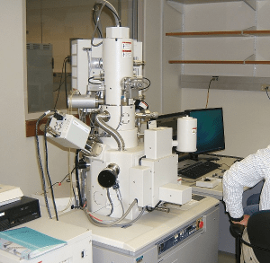
About the instruments
Two Hitachi SU-70 scanning electron microscopes provide 1 nm resolution with a high-brightness electron source. Both SEM instruments accelerate electrons from 0.5 to 30 kV, and are equipped with an energy filtered BSE detector above the objective lens. One of the microscopes (“R2D2”) has an energy dispersive x-ray detector for elemental analysis, while the other (“C3PO”) is equipped with a solid-state backscatter detector for enhanced imaging of grain boundaries. Dual objective magnets allow the user to switch between field-immersion and non-field modes.
Available to Yale researchers & external researchers
Specifications
| Accel. voltage | 0 to 30 kV |
| Resolution @30kV | 1 nm |
| Max sample size | 10cm dia. x 1cm high |
Rates
Rates in US$/hour unless otherwise noted
| Yale academic | External academic | Industrial | |
|---|---|---|---|
| SEM, Hitachi | 37 | 61 | 215 |
| AFM, Bruker | 35 | 58 | 105 |
| e-beam, EBPG | 100 | 165 | 300 |
| TEM, FEI Osiris | 100 | 165 | 300 |
| Ion mill, Fischione | 37 | 61 | 111 |
| Ion mill, Hitachi | 37 | 61 | 111 |
| Gold sputtering | 20 | 32 | 76 |
| Iridium sputtering | 20 | 32 | 76 |
| Microtome, Leica | 30 | 50 | 90 |
| HSQ resist, 4 ml | 25 ea | 41 ea | 75 ea |
| CSAR resist, 4 ml | 20 ea | 33 ea | 60 ea |
| Dektak profilometer | 10 | 16 | 45 |
Training & services
We have recorded a set of video clips for SEM training. You will be at the SEM, watching and copying the videos, while the instructor is nearby and available for questions. You will stop the videos at various times so that the instructor can check your progress. This seems to work pretty well, and people like going through the course at their own pace. You might take one hour, or you might take four hours. It’s up to you. Sign up for SEM training by using SEM training@YINQE PPMS.
Contact
SEM prep tools
Cressington 208 iridium sputtering tool
Iridium is useful for coating samples before electron microscopy. The Cressington 208 iridium sputtering tool provides very smooth, conformal coatings which are free of the grain structure found in films of Au or Au-Pd. Chromium would also be a good choice for coating SEM samples, but iridium oxidizes much more slowly, and so has an advantage over fine-grained chromium films.
A sputter coater for gold is located next to the chromium system. Gold is used for coating electron-beam resist before lithography, but is not a good choice for SEM samples.
Hitachi IM4000 ion mill
The Hitachi IM4000 can be used for cross-sectioning samples (usually for SEM viewing) or for polishing surfaces. This ion mill uses a knife edge to mask the ion beam, creating a straight cut. The sample stage is easily reconfigured for polishing the sample, by milling at a glancing angle. The polishing mode can also be used for thinning TEM samples. Operating at up to 6kV, the ion current is much higher than that of the Fischione 1050, but the spot size is also much larger.
-
Instrument/equipment

Jasco Semi-Prep SFC-MS System
Designed for rapid isolation of complex mixtures as a two-dimensional SFC-MS system, equipped with both chiral and achiral columns.
Located within Catalysis and Separations CoreManisha Skaria
-
Instrument/equipment
Instruments
Microprobe, microscopes, diffractometer, spectrometers, and more.
Located within West Campus Materials Characterization Core -
Instrument/equipment
Waters UPLC/SFC 1- and 2D system
Designed for rapid analysis of complex mixtures, the system can be used as either a stand-alone SFC-MS or as a two dimensional system.
Located within Catalysis and Separations CoreManisha Skaria